parylene
Application in MEMS and semiconductor products
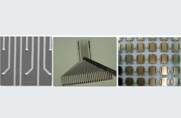
Parylene's vacuum vapor deposition process is not only similar to the manufacturing process of microelectronic integrated circuits, but also the Parylene coating prepared has a low dielectric constant. It can also be etched and mapped by microelectronic processing technology for remetallization, so Parylene can not only Used as a protective material, but also as a dielectric material and mask material in the structural layer. The integrated circuit chip coated with Parylene has a 25um thin-diameter connection line, and the connection strength can be increased by 5-10 times.
Parylene has no pinholes when it is 0.2um thick, and it can withstand DC breakdown voltage above 1000V when it is 5um. It is also a self-lubricating material with a very low friction coefficient. It is chemically inert and has good barrier properties. Therefore, it is used in microelectronics machinery. In the system, in addition to being used as a dielectric material, it is also used as a structural material and protective material for micro transmission mechanisms and micro valves.